Panelling PCBs with Altium Designer
Introduction
During the early stages of the production of an electronic board, the need often arises to have to make multiple versions of the same printed circuit board or simply to need to make a board consisting of several circuits.
This means creating several printed boards and therefore incurring prototyping costs that are greater than making a single printed board.
To overcome these problems, a possible solution is to place all our tests on a single panel, thus paying only once all the fixed costs attributable to the start of production. The creation of a single panel can be delegated to our supplier of printed circuit boards with the addition of a small surcharge.
It is a different story instead, if for reasons of time, or simply because we are making prototypes as a hobby, we rely on PCB suppliers, who have an online shop and who only provide an interface for the common settings and that do not have ad hoc panelling services for our needs.
In this case, it could be worthwhile creating your own panel at home and then having it made by any supplier. Obviously to create a single panel with all our circuits we must take into account different aspects such as the complexity of the circuit we want to create, the total surface area, the minimum dimensions, etc. Later in our article we will examine these aspects in greater detail.
The first step towards the creation of our panel is to use a CAD and ideally, as we say in jargon, an EDA (Electronic Design Automation) that will assist us in the various steps of the design both in the routing phase and in the CAM phase. In our example we will show how it is possible to perform panelling during the routing phase, using Altium Design as EDA.
Before starting
Altium Designer provides a complete environment, which helps the designer to build their circuits, from the diagram to the CAM. To aggregate the various parts of the design Altium uses the concept of workspace. In this space, the user defines the various projects for each part of the board. Each project can contain:
- a complete outline of its printed circuit board
- only the routing
- only the diagram
- etc.
In short, a project can be anything that logically forms part of our idea that we want to achieve.
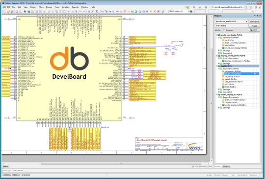
That said, let’s move on to creating a workspace for our example, where we will then add and/or create all the circuits we hope to insert in our panel. As soon as all the circuits that will be part of the panel are ready, we will create a new project that will include our panel. This will be useful when we need to generate all the necessary files for printing and assembly.
As mentioned above, to create a single panel with our circuits, various factors must be taken into consideration, and all the circuits must have:
- the same stack-up
- the same number of layers
- the same thicknesses of copper and dielectric
- similar processes (e.g. different finishes for the openings, etc.)
- constructive similarity (e.g.. blind, buried routes, etc.)
Circuit placement
Taking all these points into account, we can create our PCB project where we will also define all the construction parameters of our circuits. Obviously these parameters depend on the capabilities of our printed circuit supplier such as the maximum number of layers that the printed circuit board can have , the minimum and maximum size, the minimum size of the tracks, etc. Once all the construction parameters have been defined, it will be necessary to establish the shape of our panel, but since we have not yet placed all the circuits, we will only do this when the placement is finished.
So, as soon as we are ready, we can begin to place our circuits using the appropriate “Place > Embedded Board Array/Panelize” command:
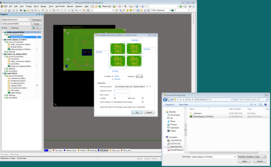
As the name suggests, the command is used to insert a circuit in our panel, in various ways:
- free placement of the single circuit
- placement with matrix layout
In the former case, the user decides where and how to place the circuit (moving it, rotating it, mirroring it), while in the latter case they decide to repeat the circuit by number of rows and by number of columns. This is very useful when we have small circuits, which we want to repeat several times on the same panel.
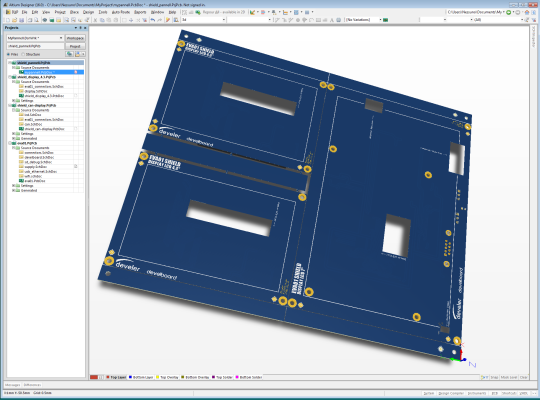
For our example, we place the circuit on our panel by hand and once only at the point we want. We proceed in the same way with all the printed boards we want to place on the panel.
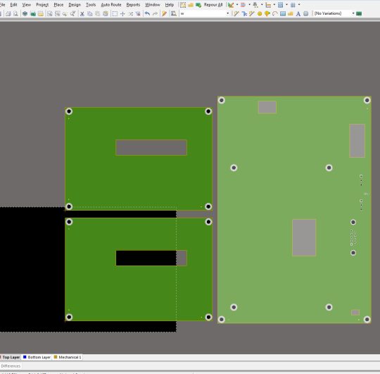
Obviously it is necessary to be careful about the process, for example, mirroring means changing the top with the bottom, and if by chance we have particular configurations of the layout of the board this could be reversed with respect to what is expected.
The placement should be performed in such a way as to minimise the empty space in order not to waste the printout, perhaps by moving or rotating the already placed circuits.
Panel finishing
As soon as we are satisfied with our placement, we can move on to adding information for the cutting of the various circuits. In fact, once the panel is built, we should have an easy way to separate the individual circuits without damaging the individual prints.
To facilitate the separation of the various prints there are various techniques:
- engraving of the printed board (scoring)
- milling
The first method consists of the V-cut incision of the printed board via tool. Engraving the printed board “weakens” it and facilitates splitting by bending. This technique is indicated when the shape of the boards is regular and the boards are joined on straight sides and without discontinuity.
The second, instead, consists of a clean cut of the printed board by means of a cutter and, in order to keep the various circuits together, some points are left where the printed board is not removed. In this way, the printed boards are already divided except for these “points” of fixing, called tap route. In general, tap route are used when the contours of the printed board are not regular but have curves, diagonals or etc. Also in this case separation takes place by splitting or by cutting with dedicated tools. To facilitate the separability of the printed boards, holes are added at the contact points to weaken the resistance to splitting.
The choice of which of these techniques to use also depends on a number of considerations:
- if the boards are mounted by machine, the use of scoring makes the printed board more immune to vibrations and more stable, but if the board has an irregular shape, it cannot be used;
- when the printed board is irregular, it is preferable to mill and use the tap route, seeking to add sufficient supports to hold the printed board with the aim of reducing vibrations in the case of machine assembly.
The two techniques are obviously not exclusive but they can both be used on the same printed board, as we will demonstrate in our example.
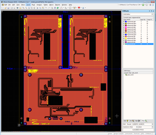
At this point, we simply have to choose how to separate the boards and report this information on the gerber so that the printed board supplier can understand how to proceed.
To better gather this information we add a layer called “PCB_Note”, where we will write and draw the various pieces of information.
Without this, we can draw the cutting points, bearing in mind that:
- the thickness of the lines represents the size of the cutting tool, that is: if I draw a 1mm line, the actual cut will be made with a 1mm tool. This means that the lines must be drawn beyond the edges of our circuits, otherwise the tool will take away part of our circuit;
- to make an incision, a line of the desired thickness is drawn, and it is noted that the line is an incision;
- the holes are without metallisation, so the final size of the hole is equal to the hole itself.
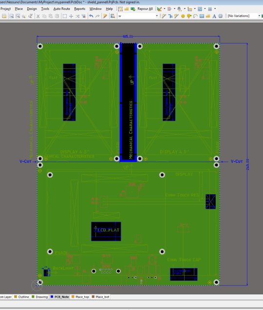
In this level we can also note other useful information for creation of the printed board such as the presence of openings, slots, or other aspects.
Further considerations
At this point, if the circuits are assembled by hand, we can complete the work by adding the finishing touches and generating the gerber. If instead the prototypes are complicated and it will be necessary to machine them then we will need to consider the following points:
- Minimum dimensions of the panel
It is necessary to check that the dimensions of your panel are large enough to be able to insert the various mechanical assembly machines (checking the minimum measurements with your supplier). - Technical rails
It may be the case that your panel can have strange shapes or be too small to be mounted with various machines. In this case it may be useful to add printed strips or bands that can support or enlarge the board. These strips are only used for machining and consequently they must be easily removed by scoring or milling. - Dense boards of components
Also, in this case, it may be useful to use technical rails, as in the previous case. - Fiducials and references
Given that assembly in the machine is automatic and computerised, the machine must have references on the printed circuit to be able to place the various components. For this reason fixed points, called “Fiducial Marks” are added, which are nothing more than signs on the printed board recognised by the machine, which can then identify the side of the board (top or bottom) and its orientation based on them. Typically these points are openings on the solder mask, generally circular in shape. The position of the fiducials and their form are described by the IPC standards, which define the standard (SMEMA FIDUCIAL MARK STANDARD). In addition to the fiducials we can add our own references, as an indication of the side or other aspects that can be useful during the assembly phases. The fiducial marks can be inserted directly on our circuit during the routing phase or, if there are technical rails, positioned directly on them, to be removed after assembly and not remaining on the circuit. In general, three fiducials are added for each side in order to make the positioning of the printed board unique to the assembly plan. In addition to the fiducials, holes will also be added on the strips to facilitate the various processes.
As in our example we will be mounting the panel in the machine we are adding technical rails and fiducials and we will conclude by defining the edge of our panel:
Conclusions
We are adding some values to achieve the dimensions of the printed board, which may be useful when we request quotes. In addition to the quotas we can add notes on the stack-up or other aspects we aim to report to the producer. In our case some circuits will have openings on the printed circuit (for the passage of flat cables), and for this reason we have inserted the correct indications.
Now we have finally concluded our panel, and through the project settings file we generate the final gerber.
A small review of the gerber…
..and send!
Thank you for your attention!